New Publication: Improving Quantum Well Tube Homogeneity Using Strained Nanowire Heterostructures

Group PhD student Nikesh Patel has just had his first paper accepted in ACS Applied Materials and Interfaces.
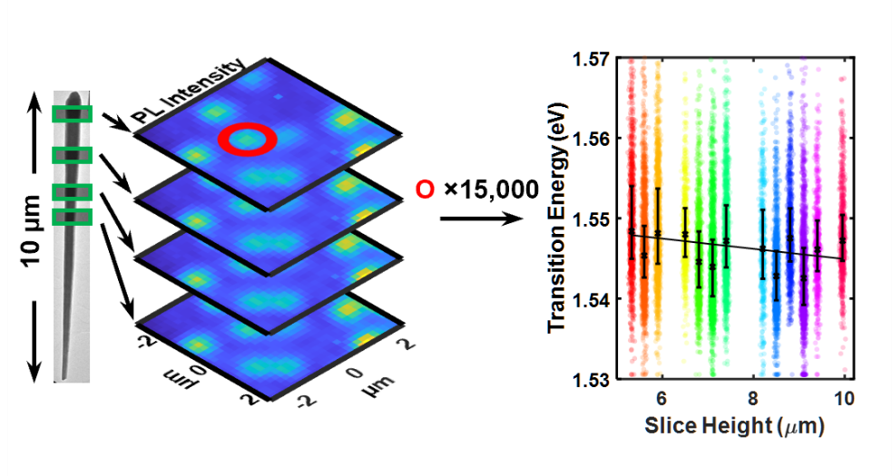
His study uses a new methodology to understand how quantum "shells" - less than 10nm thick - vary both within single nanowires, and between them. By using automated high-throughput approaches on over 15,000 nanowire sections, he shows that high uniformity is achieved through exceptional control of growth conditions but also because highly strained materials act to reduce the sensitivity to variation for a given emission thickness.
Nikesh carried out this study combining three approaches - best-in-class semiconductor nanowires grown by colleagues (Huiyun Liu and Yunyan Zhang) at UCL/National Epitaxy Facility, a cross-sectioning technique known as nanoskiving carried out by colleagues (Aruni Fonseka and Ana Sanchez) at the University of Warwick, and high throughput automated spectroscopy developed here in Manchester.
This work provided statistically rigorous assurance that high uniformity can be achieved in nanowire growth over thousands of wires, as well as giving fundamental insight into the advantages provided by highly strained systems.
This work is available now at ACS Applied Materials and Interfaces. The analysis code is available at github, and the raw data can be found at figshare.