Facilities available
The OMS lab in the Photon Science Institute hosts a number of experimental techniques. We have four areas of expertise:
- Automated/robotic high-throughput microscopy – machine vision, fast photoluminescence
- Non-linear and time-resolved spectroscopy – lasing, transient absorption microscopy
- Scanning photo-current microscopy – SPCM
- Single photon spectroscopy – iTCSPC
These techniques rely on our workhorse laser system – a PHAROS 20W, producing ultrashort pulses (200 femtoseconds) in the near infrared (1030nm) at 200,000 Hz. This is coupled with an ORPHEUS-HP optical parametric amplifier providing near gap-free tunability across 315nm to 16,000nm, with similar pulse characteristics.
Interferometeric time-correlated single photon counting
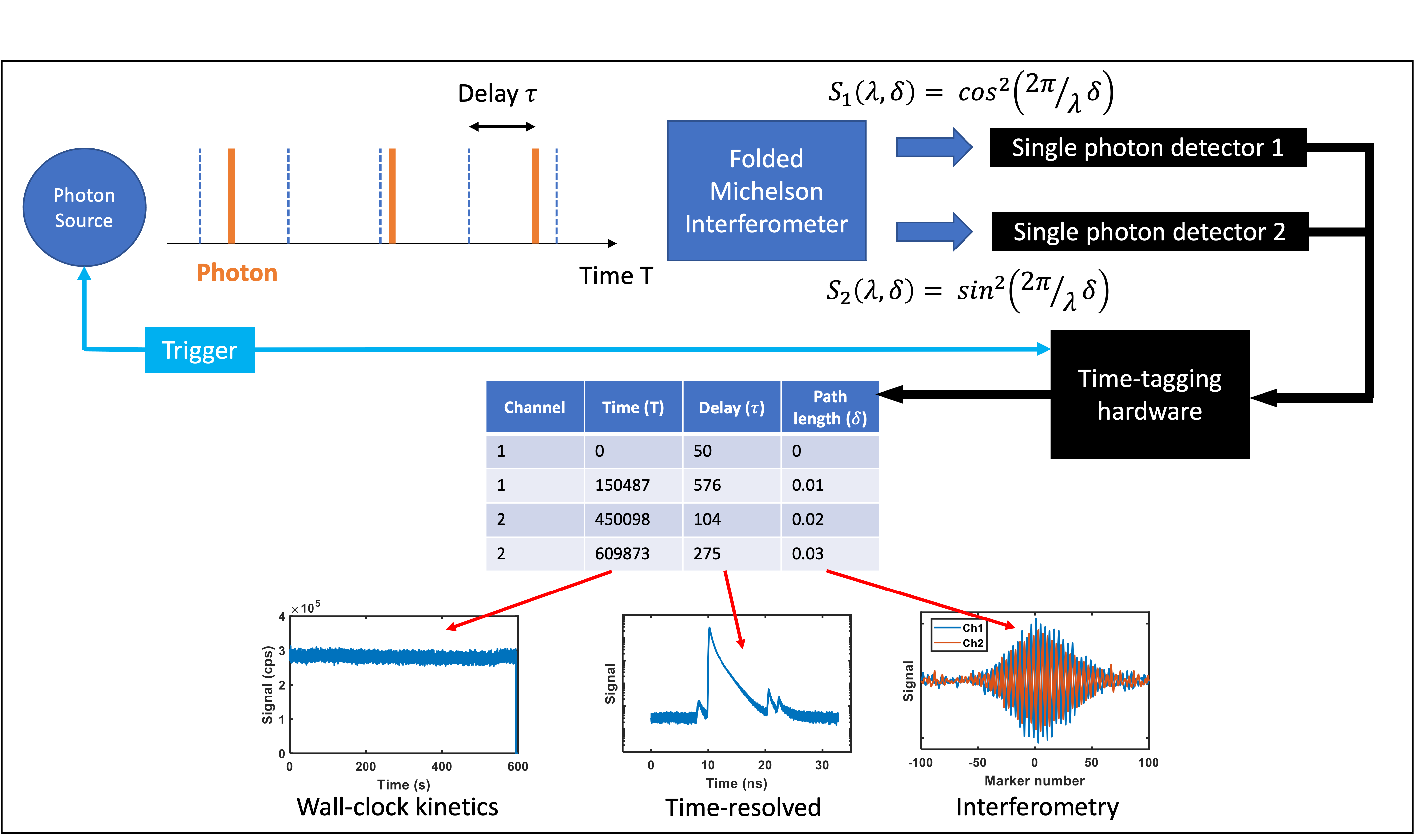
The interferometric time-correlated single photon counting system (iTCSPC) is a unique spectroscopy tool developed in the OMS lab. It combines optical interferometry – used to separate photons into one of two channels based on their wavelength – with single-photon counting – used to measure their time of arrival with picosecond (0.000000000001s) resolution.
This combination means that unlike a typical spectrometry system, every photon can be measured, towards a 100% throughput. By outputting a stream of data as the photons arrive, we can measure the arrival rate (giving brightness, or changes with time), the arrival time (giving fast delay dynamics), the variation with interferometer position (giving photon energy) and the arrival channel. The latter measure can also be used to provide quantum measurements, such as bunching/antibunching from lasers and single photon sources.
The tool is fibre coupled and can be combined with other techniques in the lab, such as microscopic spectroscopy.
Automated/robotic high throughput spectroscopy
The automated high throughput spectroscopy tool is a bespoke optical microscope system built in-house in the OMS lab which utilises state of the art translation stages to facilitate precise movements as small as 100nm, over a large travel range of 0.1m. When combined with sophisticated machine vision imaging techniques, this enables the rapid identification, location and characterisation of a wide range of nano- and micro-structures. A typical experiment can study many 10,000’s of samples in around an hour!
The tool is modular and adaptable by design, making it easy to exchange optical components to optimise the system for studying different materials (eg. Polarisers, dichroic beamsplitters, excitation filters, front/back illumination). Optically pumped experiments can be performed by directing laser beams into the system. Light collected from the samples is coupled into an optical fibre, which can then be fed into a multitude of instruments in the OMS lab for further experimental analysis (Photoluminescence, Raman, iTCSPC etc.).
High-throughput modelling
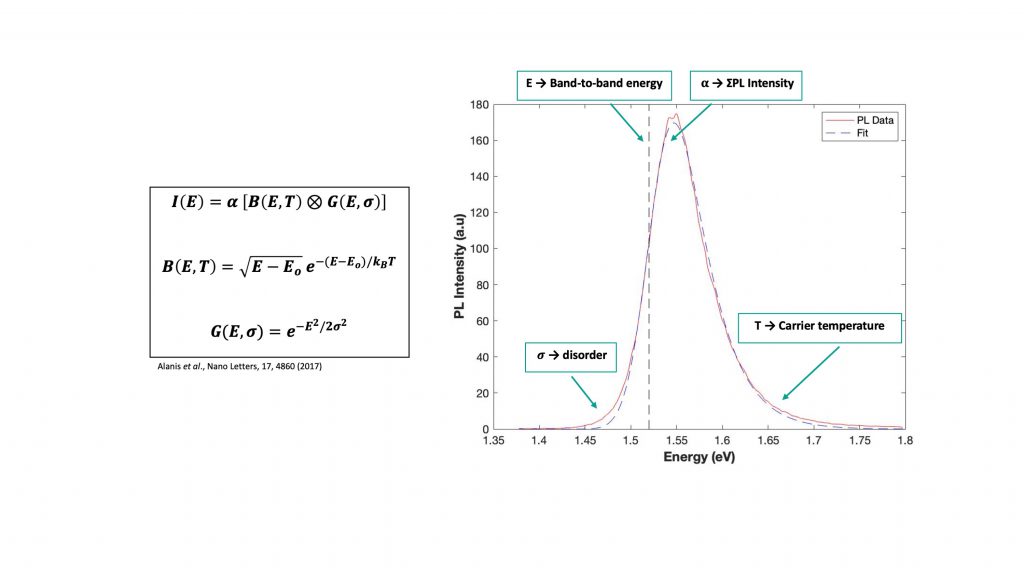
The most effective measurements from high-throughput experimentation are spectral emission – photoluminescence, electroluminescence or Raman spectroscopy. These techniques are rich in information. Modelling typical band-edge photoluminescence (PL) emission can be done in a number of ways: we prefer to use a convolution of a 3D density of states and a Gaussian distribution function multiplied by a scaling factor. Through fitting large-scale nanowires (NWs), energy band gap, carrier temperature, PL intensity, and disorder parameter related to the non-thermal contribution to the width of the PL spectrum are obtained. It is known that doping levels can be estimated from shifts in the energy bandgap, and carrier lifetimes can be estimated from the carrier temperature. In the presence of quantum wells, confinement potentials and stochiometries can be measured. Using these parameters, we can investigate the inhomogeneity between wires and link it to the functional performance of the NWs.
Scanning Photocurrent Microscopy
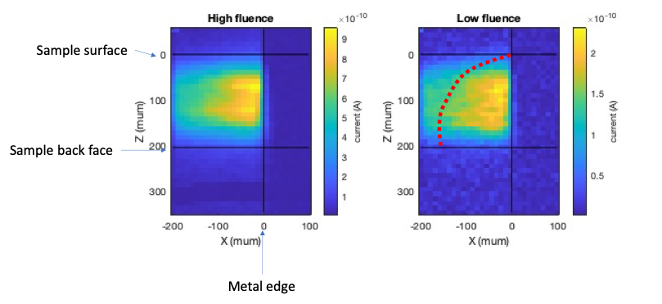
Our lab has a scanning photocurrent microscope (SPCM) to measuring the efficiency of photoconductive devices, and for investigating their behaviour under optical injection. Understanding the absorption and transport process for current is essential to improve the performance of both photodiodes (PD) and photovoltaic (PV) devices. SPCM provides the spatial dependence of device response: importantly, this includes edges and interfaces.
A variable repetition rate, high power laser is used as a light source. The laser features 450 to 16,000nm spectral bandwidth and adjustable output power up to 20W. A Lock-in amplifier (Zurich Instruments HF2LI 50 MHz) is used to measure and detect very small AC signals induced by the laser; this instrument includes a current preamplifier (ZHINST HF2TA 50 MHz) that has two input amplification channels as well as adjustable transimpedance gain ranging from 100 V/A to 100 MV/A. Devices can be biased using a Keithley instrument (6487 Picoammeter/Voltage Source) allowing an input voltage of up to 505 V. This also allows DC current measurement to the picoamp level.
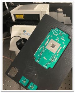
The sample itself is mounted onto a dedicated high-frequency PCB, which is attached to two scanning stages: either 300um x 300um x 300um piezo-based scanning with 1nm resolution, or 100mm x 100mm mechanical scanning with sub-micron resolution.
A voltage is injected to the PD sample and the laser induced photogenerated carriers are collected by the preamplifier. The output of the preamplifier is fed to the first input in the lock-in amplifier, while the second input is used for laser referencing that comes from the photodiode.
Characterization modes:
This SPCM provides a range of capabilities to characterize different photodetectors including:
- Photocurrent versus applied forward/reverse bias voltage for dark and illuminated photodetector device (current-voltage curve).
- Spectral response illustrating the relation between responsivity of the PD device and incident wavelength.
- Temporal response of the device using a GHz oscilliscope
- Photomapping
- Multi-photon microscopy for three dimensional mapping (also known as TOBIC).
Transient Absorption and Sum-Frequency Generation Spectroscopy
Our custom-built pump-probe setup offers capability for ultrafast transient absorption and sum-frequency generation micro-spectroscopy. It utilises the tuneable (315-16000nm) and auxilliary (1030nm and 515nm) output from the ORPHEUS-HP optical parametric amplifier, giving a range of choice for pump-probe wavelengths. We use white light continuum generation methods to create broadband pulses, and a grating diffraction compressor for IR pulse narrowing.
Samples are mounted on an automated stage, at 100 nm incremental precision, with possibility to illuminate and probe from above or below for counter-propagating geometry. Beams pass through a microscope objective, allowing microscopy experiments at sub-micron precision for bulk material, low-dimensional structures and at device interfaces. It is possible to carry out high-throughput spectroscopy with our system.
Micro-transient Absorption
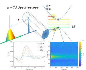
Transient absorption is a multiple photon technique that probes the induced shift in the energy level by the precedent photon. It allows to track a real time evolution of the energy states within in an extremely short timescale. (~ 100 fs or even faster) Thereby, it sheds light to the quantitative scheme of the inter/intra band charge carrier dynamics incurred by the excitation in materials.
The transient absorption spectroscopy in combine with sub-nm scale microscopy provides an unique platform to study the local carrier dynamics of noble materials heavily relying on the quantum mechanical characteristics. Thus, it manifests the nano level lattice-energy dynamics correlation which had been conventionally hidden behind the ensemble average.
Simulation capability
Nextnano
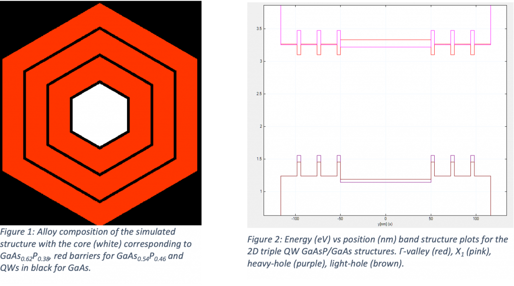
Nextnano is a simulation software package we use for the theoretical optoelectronic characterisation of low-dimensional semiconductor nanostructures. This is achieved by solving the Schrodinger equation at each point in a mesh grid for a generated structure. Nextnano provides a means to validate and understand experimental optical spectroscopy results, simulating optical and electronic properties of the structure in tandem with pseudomorphic strain, bandgap arrangement and quantum confined wavefunctions. It offers a wide range of customisability from selecting the crystal structure, alloy composition and illumination sources. The software also lets one sweep through a range of values for a parameter, such as alloy composition and structure thickness, which can justify spread in a dataset that is difficult to acquire through experimental means.