Research
Research Themes
The group has a focus on the use of cutting-edge and novel experimental optical and electronic techniques to study micro- and nanomaterials with an optoelectronic application. This interest spans:
- highly-integrated microLED arrays
- 2D materials and devices
- semiconductor nanowires
- emerging photovoltaic and photosensitive materials
We study these systems using home-built high-throughput automated experimentation, correlative methods and data-led materials analysis to provide statistically rigerous understanding.
If you are interested in collaboration or pursing a PhD in this field, please get in touch.
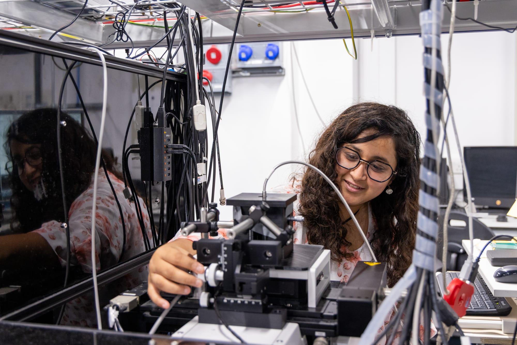
High-throughput and automated methods
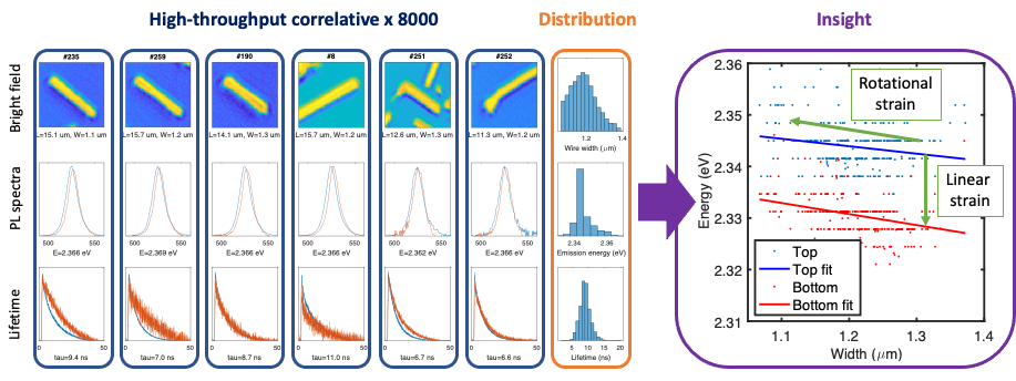
By measuring more than one object of a given material, we can learn more about the material. This can be as simple as distributions in properties or performance such as yield measurements, where we might want to design for narrow distribution. We can also use high-throughput to identify the best-in-class sample, which can provide information on the limits of performance.
However, the most powerful application for high-throughput acquisition is to correlate materials properties, such as geometry, material quality or performance, to produce a model that captures the critical limiting factor for a specific device. This is particularly useful for nanomaterials, where a large surface-to-volume ratio and challenges with geometric control at the smallest length-scales can lead to a large spread in performance.
Our implementation of high-throughput measurement couple:
- Machine vision microscopy to identify possible nano-objects with registered locations recorded
- Automated spectroscopy to measure emission or absorption
- Go/no-go decision based on imagery, spectra etc.
- More complex or time-consuming measurements, such as time-resolved spectroscopy, Raman spectra of each object or non-linear optics
- Correlative off-line measurements including SEM, TEM, AFM using registered positions
Semiconductor nanowire optoelectronics
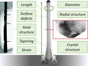
Semiconductors play a key role throughout the field of optoelectronics, providing the active material for photodetectors, light-emitting diodes, and diode lasers. Whilst materials such as silicon are commonly used, a push towards higher speed, lower cost and more tightly integrated devices have led researchers to consider novel material systems with more tunable material properties. Of particular interest are semiconductor nanowires based on III-V materials such as GaAs, InP or InAs, or perovskite nanowires such as CsPbBr or MAPI.
Nanowires inherently feature nanoscale dimensions, bottom-up fabrication routes and tuneable material parameters through surface or heterostructure engineering, and have been identified as key components for future nanotechnology-enabled optoelectronic devices. However, nanowire-based optoelectronics are a new field, and significant challenges remain for both material characterisation and optoelectronic-relevant testing.
This project is in collaboration with the nanowire growth groups at the Australian National University, University College London, the Weizmann Institute, and Lund University, and has four main goals:
- To investigate key material parameters using an integrated range of ultrafast optical techniques, including photocurrent microscopy, photoluminescence microscopy, terahertz photoconductivity, and non-linear optical approaches and correlate these measurements for deeper insight
- To understand inter-wire inhomogeneity
- To implement the best performing nanowire devices based upon the material parameters determined earlier in the project.
Relevant publications:
- Nanowire statistics: Alanis et al, Nano Letters 17, 4860
- Nanowire terahertz detectors : Peng et al, Nano Letters 16, 4925
- Nanowire lasers : Saxena et al, Nature Photonics, 7, 963 and Skalsky et al., Light: Science and Applications, 9, 43
- Nanowire quantum well systems : Davies et al, RSC Nanoscale, 7, 20531
- Nanowire inhomogeneity : Al-Abri et al., J Phys Photonics, 3, 022004
- Nanowire doping : Alanis et al., Nano Letter 19, 362
Ultrafast photodetectors

High speed detectors are essential across a number of fields. In particular, detectors based on InGaAs are essential for telecommunications, where speed directly leads to higher communication rates. At present, mature technology has built up on either silicon in InGaAs on InP architectures, both with advantages in production and implementation.
However, to go beyond the spectral ranges where these materials work – for instance, into the infrared – new materials must be used. Such wavelength ranges are important for either thermal or chemical sensing application.
Working with Tim Echtermeyer in the School of Electrical and Electronic Engineering at the University of Manchester, our group has been using our experience in ultrafast laser microscopy to develop new photodetectors based on 2D materials.
Related Publications:
- Photocurrent enhancement at edges: Unsuree et al., 2D Materials, 6, 041004
- Substrate modification for photodetectors: Selvi et al. Nanoscale, 10, 3399
- Graphene Schottky-Diode Detectors: Selvi et al. arXiv:1807.00225
Novel photovoltaic materials
Third-generation photovoltaics promise high efficiency, low cost and easily produced solar cells based upon low-temperature or roll-to-roll preparation methods. Key examples include dye-sensitised solar-cells, nanowire-based photovoltaics, colloidal quantum dot sensitised photovoltaics and the rapidly emerging field of perovskite-based devices. These materials are promising due to their use of novel materials or nano/meso-structuring to control the light absorption, charge generation and charge collection processes.
A key aspect of nano or meso-structured devices is the inhomogeneity inherent to such structuring, with critical energy processes occurring at spatially separated positions in three dimensions. Investigation can be hindered by the material in a full device performing differently from the active material alone; we therefore require a non-contact, in-situ probe of photon absorption, charge generation and charge migration processes that is sensitive on the shortest length scales and fastest time scales.
This project will address this challenge by use of recently developed and proof-of-concept techniques in time-resolved microscopy and nanoscopy, utilising visible and terahertz radiation to probe the ultrafast energy dynamics in next generation solar cells.