New Publication: Bottom-up, chip-scale engineering of low threshold, multi- quantum well microring lasers
Computation with light instead of electricity will increase speed and energy efficiency. We show a route to growing lasers directly onto chips with high repeatability to enable this technology.

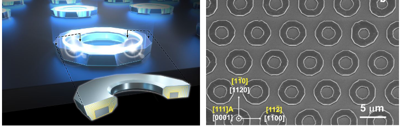
A new paper, led by collaborator Wei Wen Wong (Australian National University) was published in ACS Nano. In a major collaborative work between the Australian National University, Monash University, The University of Technology Sydney and the University of Manchester, Wei described the design, growth, and characterization of chip-scale microring lasers with application in photonic integrated circuitry.
Photonic integrated circuitry has rapidly advanced over the past decade, where light guiding, manipulation (switching) and detection are included on a single chip. The goal of this field is towards high speed, low energy, and potentially analogue or quantum computing. However, incorporating a laser directly onto the circuit has proven difficult, and external laser devices are typically used.
In this work, we show that a type of microring laser known as "selective-area grown" can provide high-yield, infrared lasing with low threshold at the chip scale. This work paves a route towards fully-integrated photonic circuitry.
Reference: Bottom-up, chip-scale engineering of low threshold, multi- quantum well microring lasers, Wong et al., ACS Nano, ASAP 2023